TPA311x series analog input audio power amplifier is a small and medium power Class D audio power amplifier product launched by Texas Instruments. This product has SpeakerGuard ™ protection function and excellent EMI performance. It is very suitable for use in products such as flat-screen TVs and iPhone Docking. This article analyzes the principles and solutions of common POP sounds in combination with practical applications.
Pin Configuration and Functions

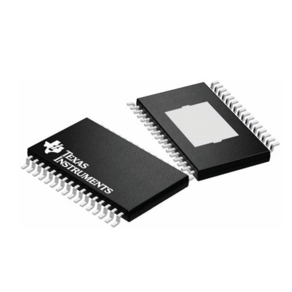
TPA3116D2 15W, 30W, 50W with AM interference suppression
Filter-free Class D Stereo Amplifier Series
Features
– 2 × 30 W Into a 8-Ω BTL Load at 24 V (TPA3118D2)
– 2 × 15 W Into a 8-Ω BTL Load at 15 V (TPA3130D2)
– DAD (32-Pin HTSSOP Pad Up)
– DAP (32-Pin HTSSOP Pad Down)
Applications
The TPA31xxD2 series are stereo efficient, digital amplifier power stage for driving speakers up to 100 W / 2 Ω in mono. The high efficiency of the TPA3130D2 allows it to do 2 × 15 W without external heat sink on a single layer PCB. The TPA3118D2 can even run 2 × 30 W / 8 Ω without heat sink on a dual layer PCB. If even higher power is needed the TPA3116D2 does 2 × 50 W / 4 Ω with a small heatsink attached to its top side PowerPAD. All three devices share the same footprint enabling a single PCB to be used across different power levels.
The TPA31xxD2 advanced oscillator/PLL circuit employs a multiple switching frequency option to avoid AM interferences; this is achieved together with an option of either master or slave option, making it possible to synchronize multiple devices.
The TPA31xxD2 devices are fully protected against faults with short-circuit protection and thermal protection as well as overvoltage, undervoltage, and DC protection. Faults are reported back to the processor to prevent devices from being damaged during overload conditions.
Reference Citations in Text
( TI, TPA3116D2 data sheet, product information and support | TI.com, https://www.ti.com/product/TPA3116D2)
Startup and shutdown timing
In order to optimize the POP sound of the switch and avoid the false trigger of the DC Detect function, it is necessary to pay attention to the startup timing of the main chip and the TPA311x device during system design. The startup sequences are divided into power sequence and enable sequence. The power sequence refers to the sequence of power supply or power off of various chips in the system. The enabling sequence can be understood as the sequence of enabling device functions determined by the system master after the system power supply is stable.
For power supply timing, since the audio output of most main chips is not stable during power-up and power-down, the ideal power-up sequence is that the system main chip powers up before TPA311x. Then TPA311x's PVCC is powered again. The ideal timing of power-off is just the opposite. The power supply for TPA311x is cut off first, and then the power supply to the main control chip is cut off.
However, the PVCC of TPA311x is usually taken from the main power supply of the system. This power supply is usually output first after the system is turned on. Afterwards, the main chip is powered by DC / DC or LDO buck. Therefore, the TPA311x is normally powered and started before the main chip is stable. In this design, the / SD pin of TPA311x must be kept low when powering up to avoid the POP sound output during the power-up of the main chip. When power is off, the TPA311x also needs to be placed in standby state to avoid the POP sound output when the main chip is powered off. Usually the POP sound during the power-on process is easier to solve, but the system needs to use a power-down detection circuit to force the TPA311x / SD to be pulled down quickly to solve the problem of power-down POP sound.
Enable timing: Since the offset voltage of the audio analog output of the main chip is generally established after the output is enabled, you need to keep / SD of the TPA311x pulled low, and wait for the offset voltage of the analog output of the main chip to stabilize before setting / SD Turn on the power amplifier. On the contrary, when you need to turn off the audio analog output function of the main chip, you need to pull down / SD to turn off the power amplifier, and then turn off the analog output signal of the main chip. This timing is to ensure that the bias voltage of the analog output of the main chip will not cause POP sound when the power is turned off.
Input-level model
TPA311x is a single power supply analog input Class D power amplifier. The analog input of this type of power amplifier must work at the DC BIAS point to transmit AC audio signals normally. The simplified input stage model is shown in Figure 2. The DC bias voltage of TPA311x is set at 3V.

When the power amplifier is started, the bias voltage will rise from 0V to the rated bias voltage. The length of this process depends on how fast the internal bias voltage source charges the external impedance network.

The process of establishing the input bias voltage of the differential input INN and INP of TPA311x is shown in Figure 3. If the differential input voltage of the differential input N and P is different, the difference will form a differential signal input amplifier and be amplified The output forms the POP sound at startup. The unbalance of the differential input bias voltage build-up process is usually due to the impedance mismatch between the input stages INN and INP. This situation is most likely to occur when the differential input is used as a single-ended input.
TPA311x single-ended input method
The analog input of the TPA311x device is a standard differential input interface. In the system design, it is recommended to use the differential input method to connect the audio output of the main chip. Using the differential input method can not only control the POP sound relatively easily, and the signal has strong anti-interference ability, but also will not cause the malfunction of the DC Detection function. The comparison between differential input mode and single-ended input mode is shown in the following table:
|
Comparison table of differential and single-ended input methods
|
||||||||
|
|
Differential input
|
Single-ended input
|
||||||
|
Anti-noise ability
|
Differential input has strong common mode noise suppression performance
|
No suppression function, need to pay more attention to PCB layout
|
||||||
|
POP sound performance at startup / shutdown
|
Differential input symmetry guarantees the most switching machine POP sound performance
|
Single-ended input requires careful design of the input network and control circuit to avoid POP sound caused by unbalanced input
|
||||||
|
DC Detect false trigger
|
Balanced differential input generally does not cause DC Delection to malfunction
|
Pay attention to the design of the input network to avoid false triggering of DC Delect during startup
|
||||||
However, in practical applications, since the audio analog output of most main chips is in single-ended mode, the differential input of the TPA311x must be configured for single-ended connection before it can be used. As shown in Figure 4, when the input is single-ended, the output of the main chip is connected to the INP pin of the power amplifier through a coupling capacitor. The INN input can be coupled to ground through a capacitor.

When using single-ended input mode, pay attention to the following points: 1. When using single-ended input mode, you need to pay more attention to the distribution of audio signal traces and ground planes, because single-ended input mode has no ability to suppress common mode interference signals in the system. 2. Compared to the differential signal input mode, single-ended input requires twice the input signal level to achieve the same output power. 3. For single-ended input mode, it is necessary to pay attention to the impedance matching of the P / N pin circuit network. Try not to use a complex filter network at the input stage. Improper impedance network will not only cause the POP sound of the switch, but also may cause the false trigger of the DC Detection function, causing the power amplifier to lock up. If you must perform filtering or gain setting at the input stage, please refer to Section 2.5 Using Op Amp for Filtering and Gain Adjustment. 2.4 Matching of input impedance network If single-ended input is used to connect to TPA311x, attention must be paid to the matching of input impedance network. As shown in Figure 5, the external impedance of the INN input of the power amplifier is Zn, usually Zn is the coupling capacitor. The output impedance of the main chip is generally very small, it can be considered that the output impedance is zero, then the external impedance of the INP input is about Zp. The internal bias voltage is gradually established when the power amplifier is started, and the process is to charge the Zn and Zp impedance networks. If the impedance difference between Zn and Zp is too large, a large differential signal will be formed between INN and INP, and this differential signal will form a POP sound after being amplified by the power amplifier. The startup time of the TPA311x amplifier design is 14mS, which is the time from / SD being pulled high to the output of the amplifier's sound. If the charging stabilization time for the input impedance network at the above start-up is less than 14mS, the differential input due to impedance mismatch will not be amplified and cause POP sound problems. Reducing the capacitance parameters in Zn and Zp can shorten the input stage settling time, but reducing the capacitance will reduce the low-frequency gain, and users need to consider it as appropriate.

Use op amps to establish isolation systems
In some systems, the audio signal output of the main chip not only needs to be connected to the power amplifier input, but also to the Line Out (line output), or other chips for processing. In this case, the input stage network is more complicated, and impedance matching in single-ended input mode is not easy to achieve. In order to solve this problem, an op amp can be used as a simple follower to establish an isolated impedance input system. The input impedance of the follower is very high and has no effect on the source signal. Its output impedance is very low, which can well match the input impedance network of TPA311x.
Figure 6 shows a circuit that uses a follower to establish an isolated input impedance network. When needed, the op amp can also be used to adjust signal gain and filtering.
TPA311X Pop sound analysis and solution
Reasons for POP and debugging methods There are two possible causes for the pop sound of TPA311x: input impedance mismatch and unreasonable system timing input impedance mismatch: input impedance mismatch will cause a voltage difference at the differential input terminal when the device is turned on and off, This POP sound is generated when the / SD voltage changes, and it occurs during the establishment of Bias (bias voltage) at the input of TPA311x. This kind of POP sound can be solved by following the method of matching the input stage impedance network in section 2.2. Unreasonable system timing ZHCA4228 TPA311x audio amplifier POP noise analysis and control As described in Section 2.1, when the main chip is turned on or off, the analog output bias voltage also needs a process of establishment, and the main chip may also output during power-up Uncontrollable POP sound. Therefore, during power-on, the power amplifier must be in Standby state. Avoid amplifying and outputting the POP sound generated by the previous chip to the speaker. The final performance of the POP sound is the same, but the root cause may be different. The following is the recommended debugging method to find the cause of the POP sound: 1. Isolate the amplifier input and the main chip output; after the POP sound appears, first disconnect the output of the main chip , And short circuit the power amplifier input circuit to ground through the capacitor AC. At this time, you can control the / SD pin level to simulate the power on and off process. If the POP sound is still present, it means that the charging speed of the P / N pin to the external network is inconsistent when the power amplifier is started, resulting in a voltage difference between the differential inputs. If the POP disappears, you can proceed to the next verification. 2. After confirming that there is no POP sound from the switch when the amplifier has no input, you can use an external power supply to power the main chip. Keeping the main chip power supply not cut off is to eliminate the influence of POP sound when the main chip output is powered off. At this time, the normal system power-on and power-off verification POP sound is performed. If the POP sound is eliminated, it can be judged that the power-off timing of the main chip and the power-off timing of the power amplifier do not match, causing the POP sound generated when the main chip is powered off to be amplified and output by the power amplifier. In some systems, the power is not completely turned off. When the system has a standby mode, the I / O port of the standby chip can be used to control the timing. If the system's switch is in the hard power-off mode, the system power timing needs to be optimized. In some cases, it is necessary to add a power-up / power-down detection circuit to control the POP sound.
Power-off detection circuit In a system that uses a hardware switch to directly turn off the main power supply, POP sound control during power-off is more difficult. Because this type of system cannot predict the system power down in advance, it is impossible to use the controller I / O port to mute or turn off the power amplifier before power down. At this time, you must use the power-down detection circuit shown in Figure 7 to solve this problem. This circuit can provide a control signal in the early stage of the system voltage drop. Use this control signal to pull down the / SD pin to quickly turn off the power amplifier in the early stage of power failure. When the power failure detection circuit supplies power normally, PVCC will charge the large capacitance of C1 through diode D1 and resistor R1. During the initial power-down period, the base voltage of Q1 will decrease with the drop of PVCC. After dropping to the opening of Q1 transistor, the voltage of C1 will be sent to the base of Q2 through Q1, Q2 will be turned on, and / SD will be pulled down.
Focus on Audio
Leave a comment
This site is protected by hCaptcha and the hCaptcha Privacy Policy and Terms of Service apply.